Message boards : Graphics cards (GPUs) : GTX 590 coming?
| Author | Message |
|---|---|
|
Hypernova  Send message Joined: 16 Nov 10 Posts: 22 Credit: 24,712,746 RAC: 0 Level Scientific publications | |
|
It seems we may get in February a new card the GTX 590 that will be a dual 580 card. All cores (1024 total) will be active but frequencies a little lower to cut consumption and heat. It will be interesting to see how they will behave on GPUGrid. | |
| ID: 20327 | Rating: 0 | rate:
| |
 Carlesa25 Carlesa25Send message Joined: 13 Nov 10 Posts: 328 Credit: 72,619,453 RAC: 23 Level Scientific publications | |
|
Español: | |
| ID: 20329 | Rating: 0 | rate:
| |
|
skgiven Volunteer moderator Volunteer tester  Send message Joined: 23 Apr 09 Posts: 3968 Credit: 1,995,359,260 RAC: 0 Level Scientific publications | |
|
It will allow some single PCIE slot users to basically have 2 GPUs, and dual slot users to have more than 2 GPUs. Good news. My guess is that they will be slightly more energy efficient than the GTX580 cards (performance per Watt). Hopefully they will drive the price of other cards down too; the GTX580 is still far too rich for many, and if the GTX570 is only the 3rd fastest Fermi then those prices may see an early fall too. | |
| ID: 20331 | Rating: 0 | rate:
| |
|
Hypernova Send message Joined: 16 Nov 10 Posts: 22 Credit: 24,712,746 RAC: 0 Level Scientific publications | |
Español: You are right. You won't have 1024 Cores available only for one task. It will be two GPU at 512 core each, and crunching each one a separate task. The reason I was mentioning 1024 cores, was to say that Nvidia had to arbitrate for consumption and thermal reason, to either reduce the number of active cores per GPU or reduce the frequencies. In my opinion the fact that they preferred to keep all cores active, is I think the better variant for crunching. For game playing were framerates (fast cycle times) are paramount, probably choosing to keep frequencies high would have been best. But maybe I am wrong. | |
| ID: 20332 | Rating: 0 | rate:
| |
|
skgiven Volunteer moderator Volunteer tester Send message Joined: 23 Apr 09 Posts: 3968 Credit: 1,995,359,260 RAC: 0 Level Scientific publications | |
|
AMD will be showcasing Bulldozer and Antilles at CeBit, which will be in Hannover from 1st to 5th March this year. | |
| ID: 20351 | Rating: 0 | rate:
| |
|
ExtraTerrestrial Apes Volunteer moderator Volunteer tester Send message Joined: 17 Aug 08 Posts: 2705 Credit: 1,311,122,549 RAC: 0 Level Scientific publications | |
|
For games and regarding shaders it doesn't matter if you increase shader count or frequency. The task is "embarrassingly parallel", meaning even at just 1024x786 we've got 0.8 million pixels per frame and could to first approximation make use of just as many shaders in parallel (this number will go down by a factor of 20 or so if you consider pipeline depth, but still safe). And regarding frequency: we need frames at Hz region, whereas GPU frequencies are in the MHz region. | |
| ID: 20488 | Rating: 0 | rate:
| |
|
skgiven Volunteer moderator Volunteer tester Send message Joined: 23 Apr 09 Posts: 3968 Credit: 1,995,359,260 RAC: 0 Level Scientific publications | |
|
Anticipated release date is the 22nd March, according to several reports - only 11 days. | |
| ID: 20648 | Rating: 0 | rate:
| |
|
ExtraTerrestrial Apes Volunteer moderator Volunteer tester Send message Joined: 17 Aug 08 Posts: 2705 Credit: 1,311,122,549 RAC: 0 Level Scientific publications | |
|
Agreed - if they follow the HD6990 they can probably put out a decent dual GF110, i.e. without castrating it too much to stay within 300 W. | |
| ID: 20649 | Rating: 0 | rate:
| |
|
skgiven Volunteer moderator Volunteer tester Send message Joined: 23 Apr 09 Posts: 3968 Credit: 1,995,359,260 RAC: 0 Level Scientific publications | |
| ID: 20683 | Rating: 0 | rate:
| |
|
ExtraTerrestrial Apes Volunteer moderator Volunteer tester Send message Joined: 17 Aug 08 Posts: 2705 Credit: 1,311,122,549 RAC: 0 Level Scientific publications | |
|
LOL! | |
| ID: 20685 | Rating: 0 | rate:
| |
|
alephnull Send message Joined: 8 Jul 09 Posts: 13 Credit: 306,850,267 RAC: 0 Level Scientific publications | |
|
hopefully these come out soon. i was waitin for them but when it got delayed again my patience ran out and just got the 580s. anyone have guesstimations on what the 590s may go for? i feel a second mortgage comin in the near future... | |
| ID: 20691 | Rating: 0 | rate:
| |
|
skgiven Volunteer moderator Volunteer tester Send message Joined: 23 Apr 09 Posts: 3968 Credit: 1,995,359,260 RAC: 0 Level Scientific publications | |
|
You're about right on the cost - mortgage territory. | |
| ID: 20692 | Rating: 0 | rate:
| |
|
skgiven Volunteer moderator Volunteer tester Send message Joined: 23 Apr 09 Posts: 3968 Credit: 1,995,359,260 RAC: 0 Level Scientific publications | |
|
Hexus suggest a very reasonable TDP of 365W. This might mean the 622MHz I read elsewhere (607) is real and might lay some doubt about if it will outperform a 6990. That said I still think it will be 50% faster than a single GTX580. | |
| ID: 20705 | Rating: 0 | rate:
| |
|
ExtraTerrestrial Apes Volunteer moderator Volunteer tester Send message Joined: 17 Aug 08 Posts: 2705 Credit: 1,311,122,549 RAC: 0 Level Scientific publications | |
|
Well, if you'd need a mortgage to afford one.. you probably shouldn't ;) | |
| ID: 20709 | Rating: 0 | rate:
| |
|
Carlesa25 Send message Joined: 13 Nov 10 Posts: 328 Credit: 72,619,453 RAC: 23 Level Scientific publications | |
|
Hi, My experience with a GTX295 is very good (on Linux and Windows) better than its equivalent in SLI, lower consumption and easy installation and OC quite broad, also suggests in mount 4 GPU and is not nonsense. | |
| ID: 20711 | Rating: 0 | rate:
| |
|
The dual GPU on a single card configurations have certain advantages. Ability to install in a single PCIe slot motherboard is one, but another (the one interests me, frankly) is water cooling. A single watercooling block is typically about $110-$120 or so. With proper cooling, there's little reason a dual-GF110 card won't be able to achieve full GTX580 clock speeds if your power supply can handle it. Once you factor in the costs of the waterblock(s), it might even be less expensive than two 570/580s. | |
| ID: 20715 | Rating: 0 | rate:
| |
|
skgiven Volunteer moderator Volunteer tester Send message Joined: 23 Apr 09 Posts: 3968 Credit: 1,995,359,260 RAC: 0 Level Scientific publications | |
|
Most people that buy these cards will probably remove the heatsink and fans, and go straight to water cooling. If it's TDP is only 365W and the user has a PCIE2 slot then the system can supply up to 450W to the card – plenty of headroom to overclock to at least the GTX580 ref of 772MHz, probably more saying as these will be the sweetest of cores. | |
| ID: 20718 | Rating: 0 | rate:
| |
|
skgiven Volunteer moderator Volunteer tester Send message Joined: 23 Apr 09 Posts: 3968 Credit: 1,995,359,260 RAC: 0 Level Scientific publications | |
|
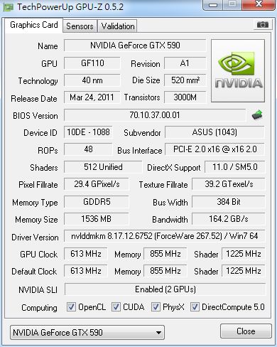
Ref specs: | |
| ID: 20778 | Rating: 0 | rate:
| |
|
There's also this review from benchmarkreviews.com | |
| ID: 20780 | Rating: 0 | rate:
| |
|
There is a major factor lurking outside the marketing/fanboy hype of both the 590 and 6990, and those considering a long term purchase of high cards may well like to consider it if not really known before. Both the 590 and 6990 are cobbled together designs patching over the cracks resulting from the 32nm fabrication being canned - they had no choice but to release new designs on 40nm. AMD were in a better position to slip the Nothern Islands design to 40nm, NVidia had a bigger hassle as it was still getting over the Fermi debacle. The result is of course two fast cards, but both are hobbled by the fact they had to go to 40nm. | |
| ID: 20787 | Rating: 0 | rate:
| |
|
skgiven Volunteer moderator Volunteer tester Send message Joined: 23 Apr 09 Posts: 3968 Credit: 1,995,359,260 RAC: 0 Level Scientific publications | |
|
Perspective, | |
| ID: 20788 | Rating: 0 | rate:
| |
|
ExtraTerrestrial Apes Volunteer moderator Volunteer tester Send message Joined: 17 Aug 08 Posts: 2705 Credit: 1,311,122,549 RAC: 0 Level Scientific publications | |
|
28 nm cards should be a lot more attractive.. but don't expect miracles! | |
| ID: 20790 | Rating: 0 | rate:
| |
|
Retvari Zoltan Send message Joined: 20 Jan 09 Posts: 2343 Credit: 16,201,255,749 RAC: 698 Level Scientific publications | |
|
The transition from 55nm to 40nm, and creating a working brand new Fermi architecture took NVidia more than a year (that was the GTX 480-470-465 line), and then another 9 months to reach the original goal of 512 shaders (GTX 580-570). Then it took them 3 months to select the chips for a twin-chip "world's fastest GPU" which is clearly made for one purpose: to gain in NVidia's prestige. If a new GPU made with the 28nm fabrication process was about to release, why would NVidia (and AMD) waste their time and resources to come up with something like the GTX 590? (which is clearly more expensive to produce than they sell it, that's why they limit it's production) | |
| ID: 20791 | Rating: 0 | rate:
| |
|
skgiven Volunteer moderator Volunteer tester Send message Joined: 23 Apr 09 Posts: 3968 Credit: 1,995,359,260 RAC: 0 Level Scientific publications | |
|
A GPU with many small efficient cores could be the answer to significantly increase crunching and server farm performance per Watt, but such cards would not sell to gamers, or be of much use as entry level GPUs. Perhaps market changes will open gateways to such cards and the development of software such as OpenCL/OpenGL will drive either NVidia and/or ATI towards such cards, in a similar way to Intel being driven towards developing a range of small efficient CPU cores for server farms. | |
| ID: 20793 | Rating: 0 | rate:
| |
|
ExtraTerrestrial Apes Volunteer moderator Volunteer tester Send message Joined: 17 Aug 08 Posts: 2705 Credit: 1,311,122,549 RAC: 0 Level Scientific publications | |
|
Well said, Retvari. I've just got to add one detail: in a new process node power the reduction in power consumption not only comes from reduced voltage. The smaller transistors usually also require less power for switching because, well, they're smaller (simply said). This adds to the voltage scaling but is difficult to predict (and TSMCs 40 nm was rather dissappointing in this regard). | |
| ID: 20794 | Rating: 0 | rate:
| |
|
skgiven Volunteer moderator Volunteer tester Send message Joined: 23 Apr 09 Posts: 3968 Credit: 1,995,359,260 RAC: 0 Level Scientific publications | |
|
What I meant is having more cores, as in the GTX590 has two cores. A card with 4, 8 or 16 might well be a better performer in terms of computational power per Watt. I'm not talking about 3Billion transistors per core though, perhaps 1B or 1.5B at 28/22nm for 8 cores. | |
| ID: 20795 | Rating: 0 | rate:
| |
|
Retvari Zoltan Send message Joined: 20 Jan 09 Posts: 2343 Credit: 16,201,255,749 RAC: 698 Level Scientific publications | |
The smaller transistors usually also require less power for switching because, well, they're smaller (simply said). Well, this is *almost* true, and a transistor is only a part of the chip. It's quite logical, that smaller transistors require less power for switching, but on a chip there are parasitic capacitors everywhere on the entire area of the chip. A capacitor's (practical or parasitic in our case, their physics is similar to each other) capacitance is in direct ratio to it's electrode's surface area, but in reciprocal ratio of the electrode's distance. So if a transistor's area is reduced, this is good. But with this reduction the transistor's semiconductor part is also gets thinner, which is bad (and also good, because it's lowers the voltage needed to switch between logical levels). Also, the wiring comes closer to each other, which is also bad. Moreover a chip built thinner litography could contain more components, connected by (overall) longer wires, which is also bad. The only way to overcome this bad factors is creating better insulation between the conductors (dielectric in terms of a capacitor). This adds to the voltage scaling but is difficult to predict (and TSMCs 40 nm was rather dissappointing in this regard). I agree with that. | |
| ID: 20797 | Rating: 0 | rate:
| |
|
Retvari Zoltan Send message Joined: 20 Jan 09 Posts: 2343 Credit: 16,201,255,749 RAC: 698 Level Scientific publications | |
|
BTW I have ordered a Gainward GTX 590 yesterday, and it will be delivered tomorrow. | |
| ID: 20798 | Rating: 0 | rate:
| |
|
GDF Volunteer moderator Project administrator Project developer Project tester Volunteer developer Volunteer tester Project scientist Send message Joined: 14 Mar 07 Posts: 1957 Credit: 629,356 RAC: 0 Level Scientific publications | |
|
We, as a lab, are waiting to buy the new 28nm cards and PCI3 bus motherboards (for parallel runs). We are expecting a factor at least 2 in performance for kepler because the Fermi core design is now mature (see g80 to g200). | |
| ID: 20799 | Rating: 0 | rate:
| |
|
ExtraTerrestrial Apes Volunteer moderator Volunteer tester Send message Joined: 17 Aug 08 Posts: 2705 Credit: 1,311,122,549 RAC: 0 Level Scientific publications | |
|
Well said again, Retvari. I think I could add some more, but don't see a need to do, especially since we'd be getting OT. | |
| ID: 20801 | Rating: 0 | rate:
| |
|
Retvari Zoltan Send message Joined: 20 Jan 09 Posts: 2343 Credit: 16,201,255,749 RAC: 698 Level Scientific publications | |
We, as a lab, are waiting to buy the new 28nm cards and PCI3 bus motherboards (for parallel runs). We are expecting a factor at least 2 in performance for kepler because the Fermi core design is now mature (see g80 to g200). This is a realistic expectation, but fifteen times as Zydor said is irrealistic. I expected that before NVidia releases kepler, they transferring the GF110 to 28nm, as they did it with the GT200 (65 to 55nm), and release a dual GPU card built on this smaller, faster, cooler, cheaper chip. But neither NVidia, nor ATI released their new dual GPUs on 28nm, so there must be some reason behind it (I mean technological difficulties at TSMC) I've found the corresponding technological articles on wikipedia (in my previous post I *almost* recalled everything right... :) http://en.wikipedia.org/wiki/Low-k_dielectric http://en.wikipedia.org/wiki/High-k_dielectric http://en.wikipedia.org/wiki/Silicon_on_insulator Light reading :) | |
| ID: 20802 | Rating: 0 | rate:
| |
|
ExtraTerrestrial Apes Volunteer moderator Volunteer tester Send message Joined: 17 Aug 08 Posts: 2705 Credit: 1,311,122,549 RAC: 0 Level Scientific publications | |
|
Easy: TSMC 28 nm is not ready yet :p | |
| ID: 20803 | Rating: 0 | rate:
| |
|
The 15x times refered specifically the Maxwell chip in 2013, which will be on 22nm. NVidia claims, not mine. I share a healthy scepticism particularly as its 2+ years away and referred to a 2013 release, not relevant to Kepler, I dont believe it impossible, guess time will tell in 2+ years. It serves to illustrate NVidia claims and direction, but is not relevant to a 590 successor. | |
| ID: 20804 | Rating: 0 | rate:
| |
|
Retvari Zoltan Send message Joined: 20 Jan 09 Posts: 2343 Credit: 16,201,255,749 RAC: 698 Level Scientific publications | |
|
My GTX590 has arrived, and I've successfully installed it into this host. More exactly I replaced the GTX480 in this host with the new GTX590. I will not overclock it for the time being. So this host has now an overclocked GTX580 and a GTX590. | |
| ID: 20806 | Rating: 0 | rate:
| |
|
skgiven Volunteer moderator Volunteer tester Send message Joined: 23 Apr 09 Posts: 3968 Credit: 1,995,359,260 RAC: 0 Level Scientific publications | |
|
Zoltan, could you post up the details here - thanks | |
| ID: 20807 | Rating: 0 | rate:
| |
|
Carlesa25 Send message Joined: 13 Nov 10 Posts: 328 Credit: 72,619,453 RAC: 23 Level Scientific publications | |
|
| |
| ID: 20809 | Rating: 0 | rate:
| |
|
Retvari Zoltan Send message Joined: 20 Jan 09 Posts: 2343 Credit: 16,201,255,749 RAC: 698 Level Scientific publications | |
Thank you! This is a reporting bug in BOINC. BOINC assumes that a streaming multiprocessor has 8 CUDA cores, which is true for G80 and G200 GPUs, but this is changed to 32 (and to 48 in CC2.1 GPUs) in the Fermi architecture. | |
| ID: 20811 | Rating: 0 | rate:
| |
|
Retvari Zoltan Send message Joined: 20 Jan 09 Posts: 2343 Credit: 16,201,255,749 RAC: 698 Level Scientific publications | |
We, as a lab, are waiting to buy the new 28nm cards and PCI3 bus motherboards (for parallel runs). We are expecting a factor at least 2 in performance for kepler because the Fermi core design is now mature (see g80 to g200). The ACEMD client is having trouble to keep the Fermi GPUs busy. I wonder how will the client keep those faster GPUs busy then? | |
| ID: 20812 | Rating: 0 | rate:
| |
|
skgiven Volunteer moderator Volunteer tester Send message Joined: 23 Apr 09 Posts: 3968 Credit: 1,995,359,260 RAC: 0 Level Scientific publications | |
The ACEMD client is having trouble to keep the Fermi GPUs busy. I take it you mean the GPU utilization percentage is low? | |
| ID: 20813 | Rating: 0 | rate:
| |
|
Retvari Zoltan Send message Joined: 20 Jan 09 Posts: 2343 Credit: 16,201,255,749 RAC: 698 Level Scientific publications | |
The ACEMD client is having trouble to keep the Fermi GPUs busy. I mean the Fermi GPU utilization is pretty much CPU speed dependant, and WU type dependant. If these factors won't change for the better in the future, then the ACEMD client will need 8GHz+ CPU cores to feed the new GPUs. | |
| ID: 20814 | Rating: 0 | rate:
| |
|
ExtraTerrestrial Apes Volunteer moderator Volunteer tester Send message Joined: 17 Aug 08 Posts: 2705 Credit: 1,311,122,549 RAC: 0 Level Scientific publications | |
I mean the Fermi GPU utilization is pretty much CPU speed dependant, and WU type dependant. If these factors won't change for the better in the future, then the ACEMD client will need 8GHz+ CPU cores to feed the new GPUs. They could always go to larger molecules, increasing the amount of work per teim step for the GPU. But lower end cards would get choked by this. MrS ____________ Scanning for our furry friends since Jan 2002 | |
| ID: 20817 | Rating: 0 | rate:
| |
|
GDF Volunteer moderator Project administrator Project developer Project tester Volunteer developer Volunteer tester Project scientist Send message Joined: 14 Mar 07 Posts: 1957 Credit: 629,356 RAC: 0 Level Scientific publications | |
|
GPU utilization is 96-98% if using only the GPU and there will be no problem at least for a couple of generations. GPU utilization is low if you don't use SWAN_SYNC or for some workunits which uses a little of CPU. This last case will be less and less important as the new application moved even this tiny bit on GPU. | |
| ID: 20818 | Rating: 0 | rate:
| |
|
skgiven Volunteer moderator Volunteer tester Send message Joined: 23 Apr 09 Posts: 3968 Credit: 1,995,359,260 RAC: 0 Level Scientific publications | |
|
It is the case that GPU's are progressing faster than CPU's, so any app that depends partially on a CPU will increasingly hinder the GPU performance, in the long run. However there is a bit more to it that brute force speed. Take for example your 2.8GHz Pent D - this 3 generation old processor is not actually as quick as a 2.4GHz IC2D (E6600). In turn a Wolfdale is about 10 to 15% faster than an equally clocked Conroe. Move on to an i3 and you see another increase in performance, and then again when you move to Sandy Bridge. These 32nm SB processors clocks well and 5GHz is not too hard to reach. By the time we move to 22nm GPU's, it will be old hat for CPU's and 5GHz will be common for high end CPUs. By then I would expect to see many app improvements, but even if there was not it would not be all doom and gloom, so long as you upgrade you CPU when you are upgrading your GPU. | |
| ID: 20819 | Rating: 0 | rate:
| |
|
Retvari Zoltan Send message Joined: 20 Jan 09 Posts: 2343 Credit: 16,201,255,749 RAC: 698 Level Scientific publications | |
|
I made a couple of experiments in the weekend, and I've concluded that pairing my GTX580@900MHz with an i3-560@3.33GHz shortens the processing time compared to my overclocked Core2Quad9560@4GHz (no wonder, the i3 has an integrated northbridge), but not as much as the Core2Quad9560 does compared to the Pentium D 820 (no wonder, it's quite old). But I still think the FPU of the Core i3 (i5, i7) is not faster than the FPU of the Core2, but the integrated northbridge boosts the performance (the lower the GPU utilization is, the higher the boost will be). Another side effect of this boost: I had to raise the voltage of the GTX580@900 to 1.083V when it was in the i3 MB, while it runs fine at 1.062V in the Core2Quad MB. | |
| ID: 20855 | Rating: 0 | rate:
| |
|
ExtraTerrestrial Apes Volunteer moderator Volunteer tester Send message Joined: 17 Aug 08 Posts: 2705 Credit: 1,311,122,549 RAC: 0 Level Scientific publications | |
|
Yes, the FP execution units in 1st generation Core i CPUs are the same as in Core 2 CPUs. But due to numerous tweaks actual hardware utilization is better (depending on load, of course). | |
| ID: 20888 | Rating: 0 | rate:
| |
|
Retvari Zoltan Send message Joined: 20 Jan 09 Posts: 2343 Credit: 16,201,255,749 RAC: 698 Level Scientific publications | |
|
I'm going on with my experiments in this weekend. This time I'm using a Core i5-2400 (3.1GHz/3.4GHz) in an Intel DH67BL MB. The GPU is a GTX580@900MHz. My experimental host has processed two TONI_AB WUs since I've changed the CPU and the MB, they took about 16.192 sec = 4h30m to finish. Now it's processing an IBUCH_1_mutEGFR, so I'll be able to compare the performance of the i3-560 and the i5-2400, when it'll finish. | |
| ID: 20889 | Rating: 0 | rate:
| |

Message boards : Graphics cards (GPUs) : GTX 590 coming?